產品描述
EVG®810 LT
Features
- Surface plasma activation for low-temperature bonding (fusion/molecular and intermediate layer bonding)
- Fastest kinetics of any wafer bonding mechanism
- No wet processes required
- Highest bond strength at low temperature annealing (up to 400 °C)
- Applicable for SOI, MEMS, compound semiconductors, and advanced substrates bonding
- High degree of materials compatibility (including CMOS)
Technical Data
| Wafer diameter (substrate size) |
| 50 - 200, 100 - 300 mm |
| LowTemp™ plasma activation chamber |
| Process gases: 2 standard process gases (N2 and O2) |
| Universal mass flow controller: self-calibrating (up to 20.000 sccm) |
| Vacuum system: 9x10⁻² mbar |
| Opening / closing of chamber: automated |
| Loading / unloading of chamber: manual (wafer / substrate placed on loading pins) |
| Optional features |
| Chuck for different wafer sizes |
| Metal ion-free activation |
| Additional process gases with gas mixing |
| High vacuum system with turbo pump: 9x10⁻³ mbar base pressure |
| Material systems that are qualified with LowTemp™ plasma activated bonding |
| Si: Si/Si, Si/Si (thermally oxidized, Si (thermally oxidized)/Si (thermally oxidized) |
| TEOS/TEOS (thermally oxidized) |
| Si/Ge for Germanium-on-Insulator (GeOI) |
| Si/Si3N4 |
| Glass (borofloat, non-alkali): Si/Glas, Glass/Glass |
| Compound semiconductors: GaAs, GaP, InP |
| Polymers: PMMA, Cyclo Olefin Polymers |
|
"Best Known Method" recipes available for users for the above and for other materials (full list available on request)
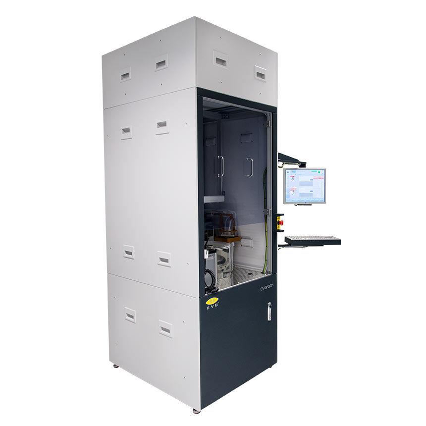
EVG®301
Features
- High-efficiency cleaning using 1 MHz megasonic nozzles or area transducers (option)
- Brush scrubbing for single-side cleaning (option)
- Diluted chemicals for wafer cleaning
- Prevents cross-contamination from back to front side
- Fully software controlled cleaning process
- Options
- Pre-bonding station with IR-inspection
- Tooling for non-SEMI standard substrates
echnical Data
| Wafer diameter (substrate size) |
| 200, 100 - 300 mm |
| Cleaning system |
| Open chamber, spinner and cleaning arm |
| Chamber: made of PP or PFA (option) |
| Cleaning media: DI-water (standard), other cleaning media (option) |
| Spinner chuck: vacuum chuck (standard) and edge handling chuck (option) made of metal ion free and clean materials |
| Rotation: up to 3000 rpm (in 5 sec) |
| Megasonic nozzle |
| Frequency: 1 MHz (3 MHz option) |
| Output power: 30 - 60 W |
| DI-water flow rate: up to 1.5 liter/min |
| Effective cleaning area: Ø 4.0 mm |
| Material: PTFE |
| Megasonic area transducer |
| Frequency: 1 MHz (3 MHz option) |
| Output power: max. 2.5 W/cm² active areas (max. output 200 W) |
| DI-water flow rate: up to 1.5 liter/min |
| Effective cleaning area: triangle shape that guarantees radio uniformity on whole wafers per each rotation |
| Material: SS and sapphire |
| Brush |
| Material: PVA |
| Programmable parameters: brush and wafer speed (rpm) |
| Adjustable parameters (brush compression, media dispense) |
|
產品圖片

圖 1

圖 2
免責聲明:以上信息由企業自行提供,內容的真實性和合法性由發布企業負責。「自助貿易」對此不承擔任何保証責任。
舉報投訴:如發現違法和不良資訊,請
點此處舉報。